← H4656 Wiring Diagram: Simplifying Your Setup Understanding amp wiring diagrams: simplifying your audio setup Trailer Wiring Protection: Best Ways to Keep It Safe! wire a trailer →
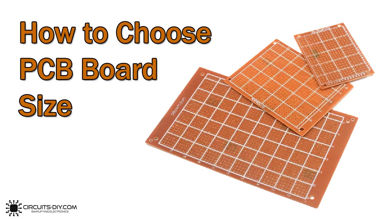
If you are looking for How to print PCB On A4 Size Paper / Print Exact Size PCB On A4 size you've visit to the right web. We have 25 Images about How to print PCB On A4 Size Paper / Print Exact Size PCB On A4 size like The Best PCB Standard Panel Sizes Guidelines for Your Design - Artist 3D, Ultimate Guide To Pcb Layout Design Considerations Mcl Images and also The Best PCB Standard Panel Sizes Guidelines for Your Design - Artist 3D. Here you go:
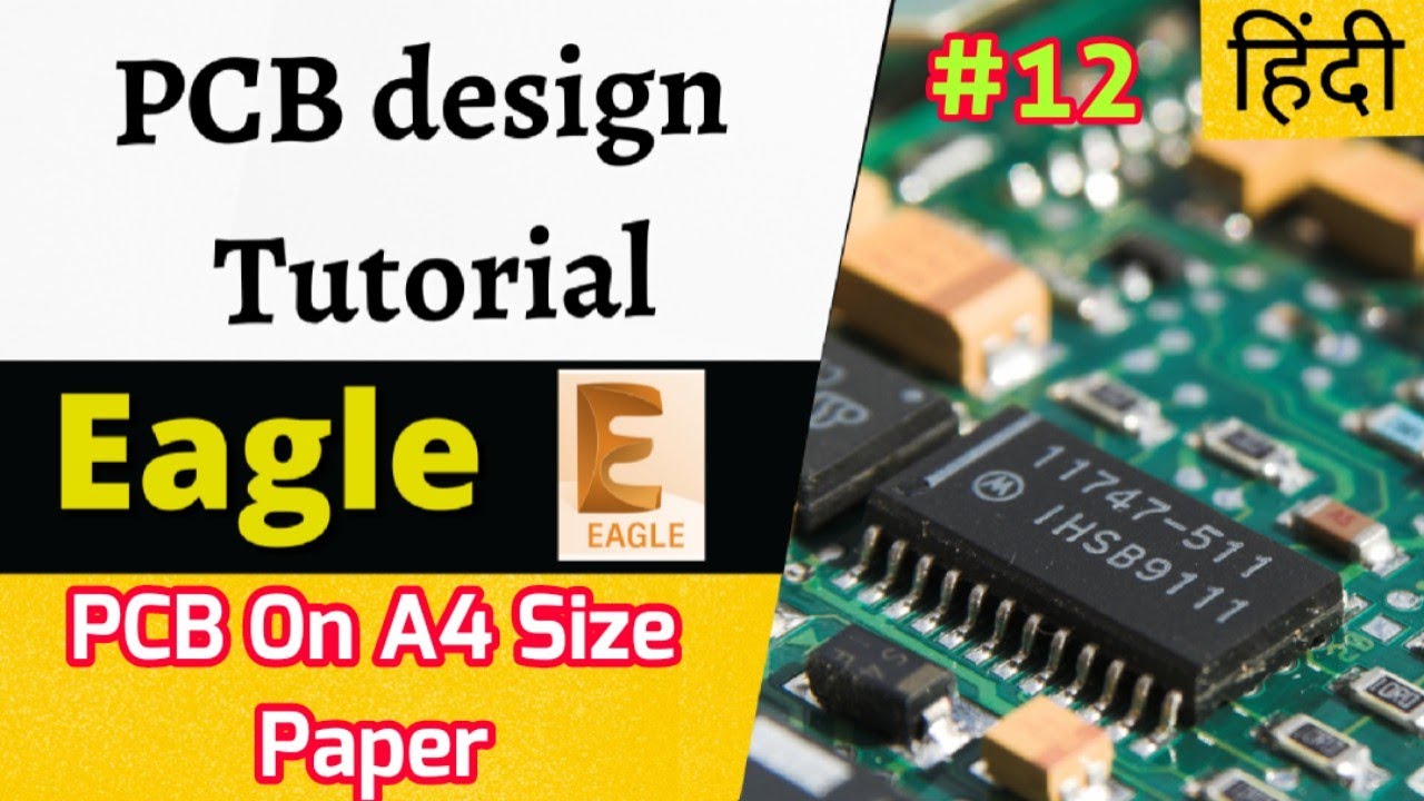
How To Print PCB On A4 Size Paper / Print Exact Size PCB On A4 Size
 www.youtube.com
How to print PCB On A4 Size Paper / Print Exact Size PCB On A4 size ...
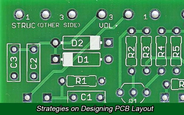
Ultimate Guide To Pcb Layout Design Considerations Mcl Images
 www.tpsearchtool.com
Ultimate Guide To Pcb Layout Design Considerations Mcl Images
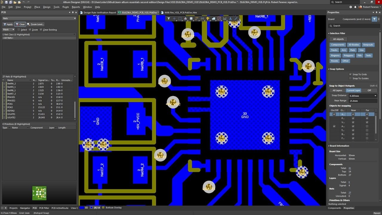
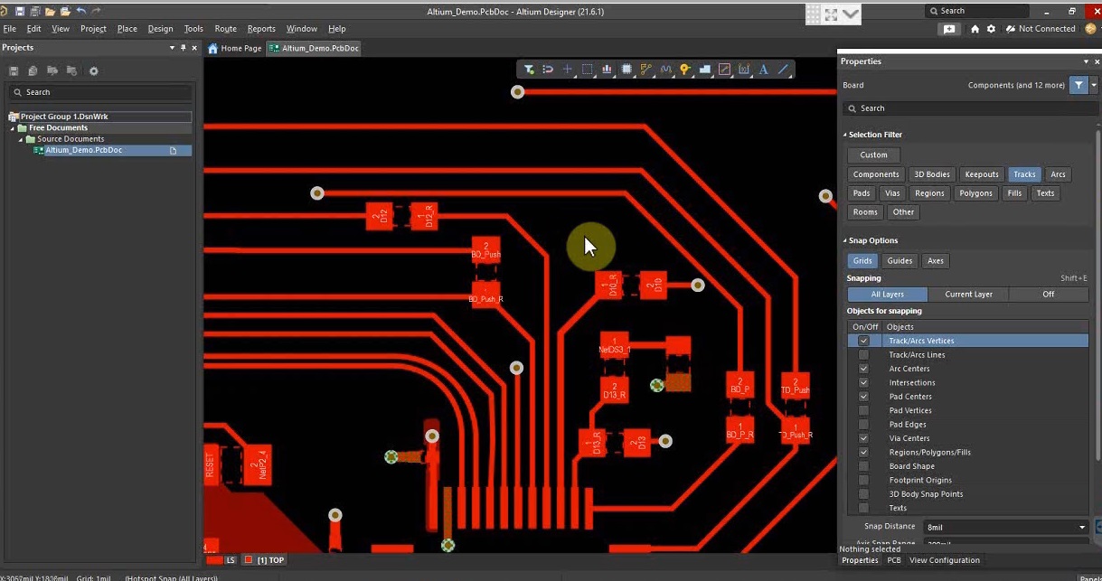
Pcb Design Using Altium
 guidemanualbevies.z21.web.core.windows.net
Pcb Design Using Altium
Ultimate Guide To Pcb Layout Design Considerations Mcl Images
 www.tpsearchtool.com
Ultimate Guide To Pcb Layout Design Considerations Mcl Images
High Speed Pcb Layout Guidelines - Design Talk
 design.udlvirtual.edu.pe
High Speed Pcb Layout Guidelines - Design Talk
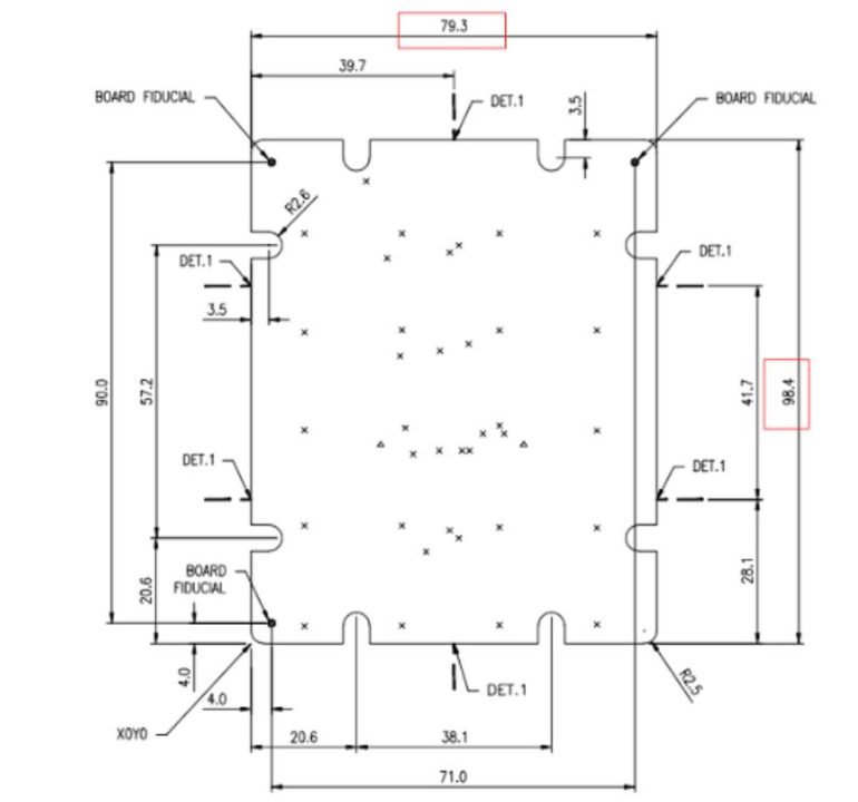
Pcb Hole Size Chart
 mavink.com
Pcb Hole Size Chart
PCB Schematic And Layout: A Comprehensive Guide – Hillman Curtis
 hillmancurtis.com
PCB Schematic and Layout: A Comprehensive Guide – Hillman Curtis ...
13 Basic Rules Of PCB Layout - Printed Circuit Board Manufacturing
 www.raypcb.com
13 Basic Rules Of PCB Layout - Printed Circuit Board Manufacturing ...
PCB Design Review And Layout Clean-Up | Sierra Circuits
 www.protoexpress.com
PCB Design Review and Layout Clean-Up | Sierra Circuits
How To Etch A PCB (Printed Circuit Board) - A Beginners Guide
 www.circuits-diy.com
How To Etch A PCB (Printed Circuit Board) - A Beginners Guide
From Origin To Future: A History Of Circuit Boards (PCB)-TechSpark
 www.tech-sparks.com
From Origin to Future: A History of Circuit Boards (PCB)-TechSpark
Mastering PCB Panelization: A Ultimate Guide For Designers
 www.elepcb.com
Mastering PCB Panelization: A Ultimate Guide for Designers
A Detailed Guide To PCB Layout Design - IBE Electronics
 www.pcbaaa.com
A detailed guide to PCB layout design - IBE Electronics
PCB Panel Size Guide: Standards, Tips & Layouts - GlobalWellPCBA
 www.globalwellpcba.com
PCB Panel Size Guide: Standards, Tips & Layouts - GlobalWellPCBA
Mastering PCB Panelization: A Ultimate Guide For Designers
 www.elepcb.com
Mastering PCB Panelization: A Ultimate Guide for Designers
O Melhor Guia Para Design De Layout De PCB - MOKO
 www.mokotechnology.com
O melhor guia para design de layout de PCB - MOKO
Tented Via: The Ultimate Guide To PCB Design And Manufacturing Techniques
 www.wevolver.com
Tented Via: The Ultimate Guide to PCB Design and Manufacturing Techniques
PCB Design Standards Of Pads Shape & Size – PCB Manufacturing And PCBA
 www.grande-pcba.com
PCB Design Standards of Pads Shape & Size – PCB Manufacturing and PCBA ...
Printed Circuit Board Layout Tutorial - Circuit Diagram
 www.circuitdiagram.co
Printed Circuit Board Layout Tutorial - Circuit Diagram
The Ultimate Guide To Electronic Design Process - HardwareBee
 hardwarebee.com
The Ultimate Guide to Electronic Design Process - HardwareBee
STM32F103C8T6 Core Board - Schematic And PCB Design | Reversepcb
 reversepcb.com
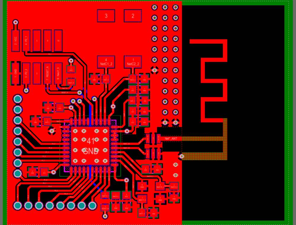
STM32F103C8T6 Core Board - Schematic And PCB Design | Reversepcb
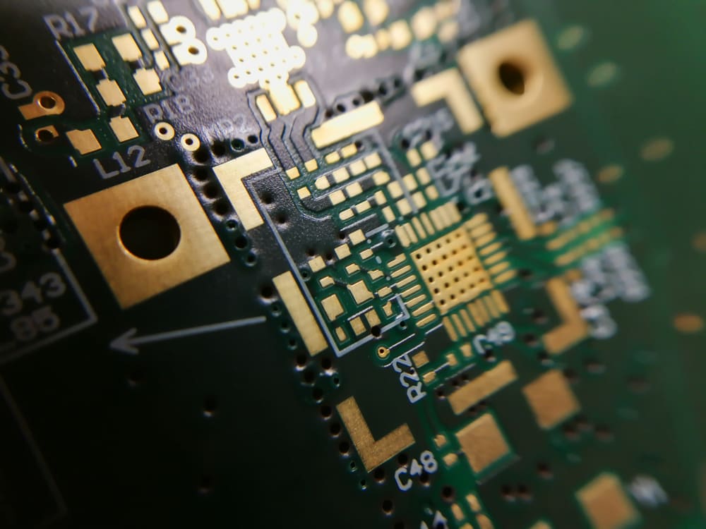
PCB Layers: Everything You Need To Know
 www.mktpcb.com
PCB Layers: Everything You Need to Know
Pcb Via Sizes
 mavink.com
Pcb Via Sizes
The Best PCB Standard Panel Sizes Guidelines For Your Design - Artist 3D
 artist-3d.com
The Best PCB Standard Panel Sizes Guidelines for Your Design - Artist 3D
A Detailed Guide To PCB Layout Design - IBE Electronics
 www.pcbaaa.com
A detailed guide to PCB layout design - IBE Electronics
pcb design review and layout clean-up. Pcb layers: everything you need to know. High speed pcb layout guidelines